- 您现在的位置:买卖IC网 > Sheet目录3822 > PIC16C66-20/SO (Microchip Technology)IC MCU OTP 8KX14 PWM 28SOIC
1997 Microchip Technology Inc.
DS30234D-page 11
PIC16C6X
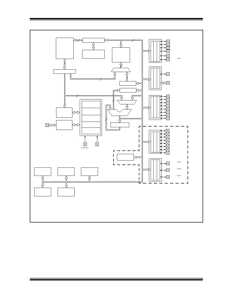
FIGURE 3-2:
PIC16C62/62A/R62/64/64A/R64 BLOCK DIAGRAM
EPROM/
Program
Memory
2K x 14
13
Data Bus
8
14
Program
Bus
Instruction reg
Program Counter
8 Level Stack
(13-bit)
RAM
File
Registers
128 x 8
Direct Addr
7
RAM Addr(1)
9
Addr MUX
Indirect
Addr
8
FSR reg
STATUS reg
MUX
ALU
W reg
Power-up
Timer
Oscillator
Start-up Timer
Power-on
Reset
Watchdog
Timer
Instruction
Decode &
Control
Timing
Generation
OSC1/CLKIN
OSC2/CLKOUT
MCLR
VDD, VSS
Synchronous
Serial Port
3
PORTA
PORTB
PORTC
PORTD
PORTE
RA4/T0CKI
RA5/SS
RB0/INT
RB7:RB1
RC0/T1OSO/T1CKI(4)
RC1/T1OSI(4)
RC2/CCP1
RC3/SCK/SCL
RC4/SDI/SDA
RC5/SDO
RC6
RC7
RE0/RD
RE1/WR
RE2/CS
RD0/PSP0
8
(Note 2)
Brown-out
Reset(3)
ROM
Timer0
Timer1
Timer2
CCP1
RA1
RA0
RA2
RA3
RD1/PSP1
RD2/PSP2
RD3/PSP3
RD4/PSP4
RD5/PSP5
RD6/PSP6
RD7/PSP7
Parallel Slave
Port
Note 1:
Higher order bits are from the STATUS register.
2:
PORTD, PORTE and the Parallel Slave Port are not available on the PIC16C62/62A/R62.
3:
Brown-out Reset is not available on the PIC16C62/64.
4:
Pin functions T1OSI and T1OSO are swapped on the PIC16C62/64.
发布紧急采购,3分钟左右您将得到回复。
相关PDF资料
PIC32MX340F128H-80V/PT
IC MCU 32BIT 128KB FLASH 64TQFP
PIC18F2610-I/SP
IC MCU FLASH 32KX16 28-DIP
PIC16F77-I/L
IC MCU FLASH 8KX14 A/D 44PLCC
PIC18F4525-I/ML
IC MCU FLASH 24KX16 44QFN
DSPIC30F2023-30I/ML
IC DSPIC MCU/DSP 12K 44QFN
PIC16LF767-I/ML
IC PIC MCU FLASH 8KX14 28QFN
PIC18LF2320-I/SO
IC MCU FLASH 4KX16 EEPROM 28SOIC
PIC18F4458-I/ML
IC PIC MCU FLASH 12KX16 44QFN
相关代理商/技术参数
PIC16C66-20/SP
功能描述:8位微控制器 -MCU 14KB 368 RAM 22 I/O RoHS:否 制造商:Silicon Labs 核心:8051 处理器系列:C8051F39x 数据总线宽度:8 bit 最大时钟频率:50 MHz 程序存储器大小:16 KB 数据 RAM 大小:1 KB 片上 ADC:Yes 工作电源电压:1.8 V to 3.6 V 工作温度范围:- 40 C to + 105 C 封装 / 箱体:QFN-20 安装风格:SMD/SMT
PIC16C66-20/SP
制造商:Microchip Technology Inc 功能描述:IC 8BIT CMOS MCU 16C66 SDIL28
PIC16C662-04/L
功能描述:8位微控制器 -MCU 7KB 176 RAM 33 I/O RoHS:否 制造商:Silicon Labs 核心:8051 处理器系列:C8051F39x 数据总线宽度:8 bit 最大时钟频率:50 MHz 程序存储器大小:16 KB 数据 RAM 大小:1 KB 片上 ADC:Yes 工作电源电压:1.8 V to 3.6 V 工作温度范围:- 40 C to + 105 C 封装 / 箱体:QFN-20 安装风格:SMD/SMT
PIC16C662-04/P
功能描述:8位微控制器 -MCU 7KB 176 RAM 33 I/O RoHS:否 制造商:Silicon Labs 核心:8051 处理器系列:C8051F39x 数据总线宽度:8 bit 最大时钟频率:50 MHz 程序存储器大小:16 KB 数据 RAM 大小:1 KB 片上 ADC:Yes 工作电源电压:1.8 V to 3.6 V 工作温度范围:- 40 C to + 105 C 封装 / 箱体:QFN-20 安装风格:SMD/SMT
PIC16C662-04/PQ
功能描述:8位微控制器 -MCU 7KB 176 RAM 33 I/O RoHS:否 制造商:Silicon Labs 核心:8051 处理器系列:C8051F39x 数据总线宽度:8 bit 最大时钟频率:50 MHz 程序存储器大小:16 KB 数据 RAM 大小:1 KB 片上 ADC:Yes 工作电源电压:1.8 V to 3.6 V 工作温度范围:- 40 C to + 105 C 封装 / 箱体:QFN-20 安装风格:SMD/SMT
PIC16C662-04/PT
功能描述:8位微控制器 -MCU 7KB 176 RAM 33 I/O RoHS:否 制造商:Silicon Labs 核心:8051 处理器系列:C8051F39x 数据总线宽度:8 bit 最大时钟频率:50 MHz 程序存储器大小:16 KB 数据 RAM 大小:1 KB 片上 ADC:Yes 工作电源电压:1.8 V to 3.6 V 工作温度范围:- 40 C to + 105 C 封装 / 箱体:QFN-20 安装风格:SMD/SMT
PIC16C662-04E/L
功能描述:8位微控制器 -MCU 7KB 176 RAM 33 I/O RoHS:否 制造商:Silicon Labs 核心:8051 处理器系列:C8051F39x 数据总线宽度:8 bit 最大时钟频率:50 MHz 程序存储器大小:16 KB 数据 RAM 大小:1 KB 片上 ADC:Yes 工作电源电压:1.8 V to 3.6 V 工作温度范围:- 40 C to + 105 C 封装 / 箱体:QFN-20 安装风格:SMD/SMT
PIC16C662-04E/P
功能描述:8位微控制器 -MCU 7KB 176 RAM 33 I/O RoHS:否 制造商:Silicon Labs 核心:8051 处理器系列:C8051F39x 数据总线宽度:8 bit 最大时钟频率:50 MHz 程序存储器大小:16 KB 数据 RAM 大小:1 KB 片上 ADC:Yes 工作电源电压:1.8 V to 3.6 V 工作温度范围:- 40 C to + 105 C 封装 / 箱体:QFN-20 安装风格:SMD/SMT